Products and Capabilities

Products and Capabilities
| Processes | Substrate Materials | Applications |
|
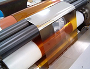
Positive and Negative Tone Resists Dual Layer Lift-off Process Etch-back Process (wet & dry) Patterning of up to 1mm thick films Front to Back Alignment Capability Roll to Roll Capability GDSII and DXF compatible |
Flexible Kapton, Mylar Rigid Glass, Polymer, Metal Aspheres |
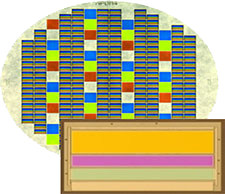
Reticles Solar Cells Filter arrays RF circuits |
| Aligner | Maximum Substrate Size | Minimum Feature Size | Registration Tolerance |
| Suss MA6 | 6" diameter x 2mm thickness | 2µm +/-0.5µm | +/-2µm |
| SPI Gen1 | 12" x 12" x 4" | 5µm +/-1µm | +/-15µm |
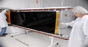
| SPI Genn II | 36" x 120" x 4" | 10µm +/-3µm | +/-25µm |
*Actual values dependent on film thickness and uniformity
Metrology and Reliability
•Cary 500 Spectrophotometer, 175 – 3300nm, -77K to 350K •Perkin Elmer 983 Spectrophotometer, 2 – 55μm
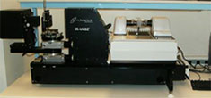
•Woollam Variable Angle Spectroscopic Ellipsometer, 250-1700nm, 2 – 33µm
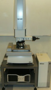
•Nikon HighResolution Microscope, ± 0.29 µm resolution
•Auto Collimator
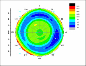
•Zygo Interferometer, λ /20 @ 633nm
•Zygo Interferometer, λ / 100 @ 1550nm
•Dektak Profilometer, 1µm to 1mm thick, 4" lateral profile
•Humidity Chamber, 5-95% RH
•Thermal Cycling Oven, 10-200C
About Us
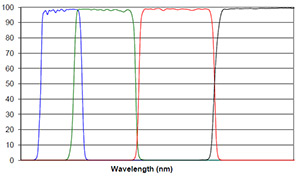
Founded in 2000 and acquired by Northrop Grumman in 2009, SPI has vast expertise and proven success in developing and providing superior thin film products to our aerospace, military, and commercial customers. Our high-precision coating capabilities span the Optical & Infra-Red (UV, VIS, NIR, SWIR, MWIR, and LWIR), and the RF spectral wavelengths to meet a vast range of applications and system needs. Utilizing advanced plasma beam and magnetron sputtering deposition techniques, SPI manufactures precision optical filters, mirror coatings, and large area magnetic and resistive films.
SPI is located in Santa Rosa, California, in the heart of wine and craft beer country. Our footprint includes 50,000 sq. ft. of manufacturing space, cleanrooms and metrology.
