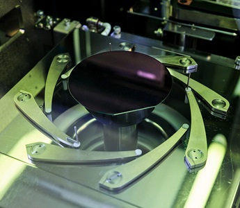
Crafted end-to-end in the USA, our next generation microelectronics ensure secure, reliable technology with unmatched precision.
Microelectronics
Powering American defense with smaller, smarter technology.
Mighty Power in the Microscopic
From superconducting and astrophysics to all the electronic charges in between, microelectronics are foundational to all advanced electronic systems. Northrop Grumman's microelectronics power advanced mission-critical systems, ensuring America leads in global military strength and innovation.
Northrop Grumman’s government accredited United States facilities consist of microelectronics experts that continue to out-invent themselves. Our microelectronics team is breaking through the laws of physics and chemistry to develop powerful next-generation systems that strengthen our national defense infrastructure.
Explore Our National Legacy in Microelectronics
Discover key locations across the United States that are integral to Northrop Grumman's storied history and lasting impact in microelectronics. This interactive map showcases our commitment to innovation and excellence nationwide.
Built with Precision. Inspired by Innovation.
Northrop Grumman’s government-Trusted American foundries and advanced packaging facilities offer limitless possibilities. Our team of world-class chemists, physicists, and engineering experts are pioneering revolutionary technologies right here in the USA.
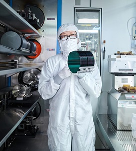
Foundry Services
Located in Linthicum, MD, Advanced Technology Lab brings over 50 years of experience in foundry services, split evenly between research and development to meet diverse customer needs.
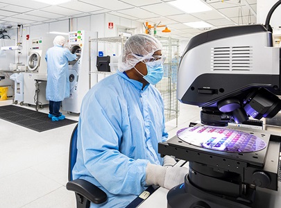
Micro-Line
Situated in Apopka, FL, our Micro-Line facility specializes in back-end wafer post-processing, providing versatile solutions for various applications.
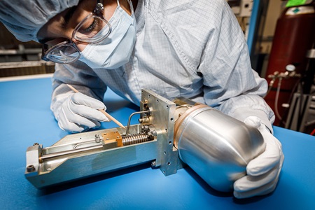
E-Band, W-Band, and Amplifiers
Based in Redondo Beach, CA, our Space Park Foundry focuses on E-Band wireless communication, W-Band applications, and high-power amplifier products.
Mighty Microelectronics Team
With over 80 U.S. patents and 49 innovation awards, our strength lies in our people, not just our tools. Our purpose-driven culture empowers employees to create groundbreaking solutions, drive continuous improvement and embrace a digital-first approach.


Tiny Tech, Mighty Mission
Tiny components such as transistors, amplifiers, regulators, sensors and switches make everything run in the defense world, and they need to be reliable.
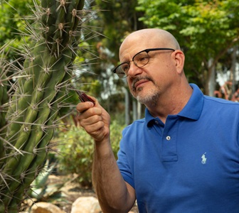
Prickly Progress
The prickly cactus plant sparked an idea to fine-tune high-tech avionics for one of the most advanced aircraft in the sky.
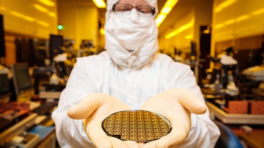
Small Components, Big Impact
At the microelectronics foundry, engineers hover over wafers that enable a range of missions, from advanced satellite communications to complex astrophysics systems.
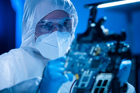
Northrop Grumman Wins CMTA’s “Coolest Thing Made in California”
Northrop Grumman’s World's Fastest Microchip has won CMTA's contest, solidifying its leadership in California's tech sector.
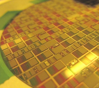
Leading U.S. Innovation with Powerful Microchips
Reviving U.S. leadership in cutting-edge technologies begins with the smallest element: the microchip.
Contact the Microelectronics Team
Have questions about how Northrop Grumman’s Microelectronics Centers can solve your toughest problems? We are here to answer them.
Telephone: 310-814-5000
